PRODUCT HIGHLIGHTS
Maximum substrate size: 8” (VPG+ 200) and 16” (VPG+ 400) respectively
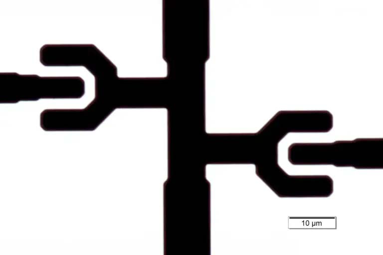
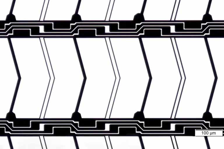
Minimum feature size: Down to 0.75 μm
Address grid: Down to 12.5 nm
Maximum write speed (at structure size 4 um): 13500 mm²/min
Exchangeable write modes
Real-time autofocus system
High power DPSS laser with 355 nm wavelength
Camera system for metrology and alignment
Closed-loop climate chamber
Automatic substrate loading system
Stage map correction
Edge detector system
Multiple data input formats (DXF, CIF, GDSII and Gerber)
Maximum substrate size: 800 x 800 mm² / 1100 x 1100 mm² / 1400 x 1400 mm²
Minimum feature size: Down to 0.75 μm
Maximum write speed (at 4 μm feature size): 16500 mm² / min
Real-time autofocus system
High power DPSS laser with 355 nm
Camera system for metrology and alignment
Closed-loop environmental chamber
Automatic substrate loading system
Stage map correction
Mura correction
Edge detector system
Multiple data input formats (DXF, CIF, GDSII and Gerber files)
曝光速度
100×100 mm²区域写入仅需9分钟
曝光质量
边缘粗糙度<40nm,CD 均匀度 <50 nm,分辨率< 500 nm
对准精度
第二层正面对准精度达 100 nm,背面 VIS / IR ±1 µm
智能对准系统
全局/局部自动对准及畸变校正;VIS 背面对准;红外(IR)对准适用于埋入结构
自动对焦
可选光学/气动对焦模式,动态补偿能力 > 160 µm
集成计量功能
实时监测位置、CD及边缘粗糙度
写入的稳定性
集成环境计量、流场控制箱和软件修正功能,以补偿环境变化

AVAILABLE MODULES
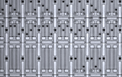
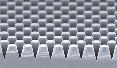
Micro-optics
MEMS
Display
Micro sensor
Micro-optics
MEMS
Display
Micro sensor
Automatic handling options
Open frame handling with SEMI standard carriers and prealigning available for 100 to 200 mm or 200 / 300 mm standard wafers (others on request)
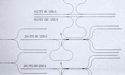
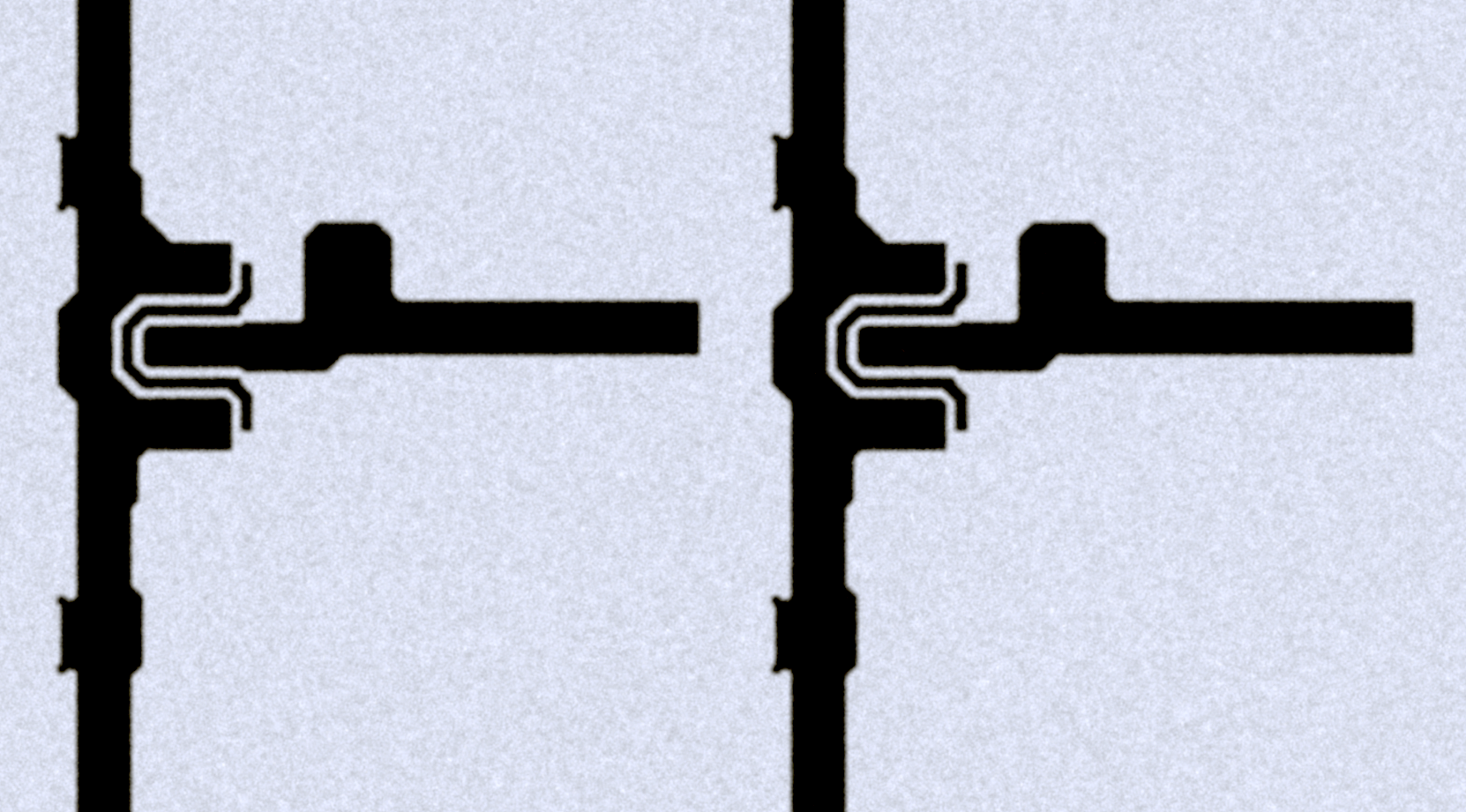
Two write modes to choose from
High NA for highest resolution or lower NA optimized for throughput or DOF critical applications
Alignment options
VIS and IR backside alignment
Service Contracts
Worldwide service level agreements for faster on-site support and access to spare parts