在高度成熟的半导体制造领域,您正面临关键挑战:如何在控制成本的同时提升产能并保持卓越品质。ULTRA半导体掩模直写系统正是为解决这一核心难题而研发,像是微控制器(MCU)、电源管理IC、LED、物联网设备、光子器件及MEMS各类芯片提供高性价比的掩模制造解决方案,以卓越的速度、精度和可靠性,助力您实现良率与盈利能力的最大化。
为什么选择 ULTRA?
ULTRA 结合最先进的技术,可解决现代掩模车间的主要问题:速度、精度和投资回报。
利用高吞吐量加快产能
ULTRA系统以超越传统设备的卓越生产力,显著减少设备停机时间,助您轻松应对紧迫的生产计划。其先进的曝光引擎和优化的写入模式,可将标准6英寸掩模版的制造时间缩短至45分钟以内。
-
基于 SLM 的快速曝光引擎:
写入速度高达 580 mm²/分钟,同时不影响质量。
-
全自动掩模版传输系统:
简化操作界面,显著降低人工干预,确保稳定可靠的掩模版装卸,实现连续生产。
-
优化的写入模式:
灵活选择速度优先或精度优先模式,精准匹配您的不同工艺需求。
以极致的精度实现最高产量
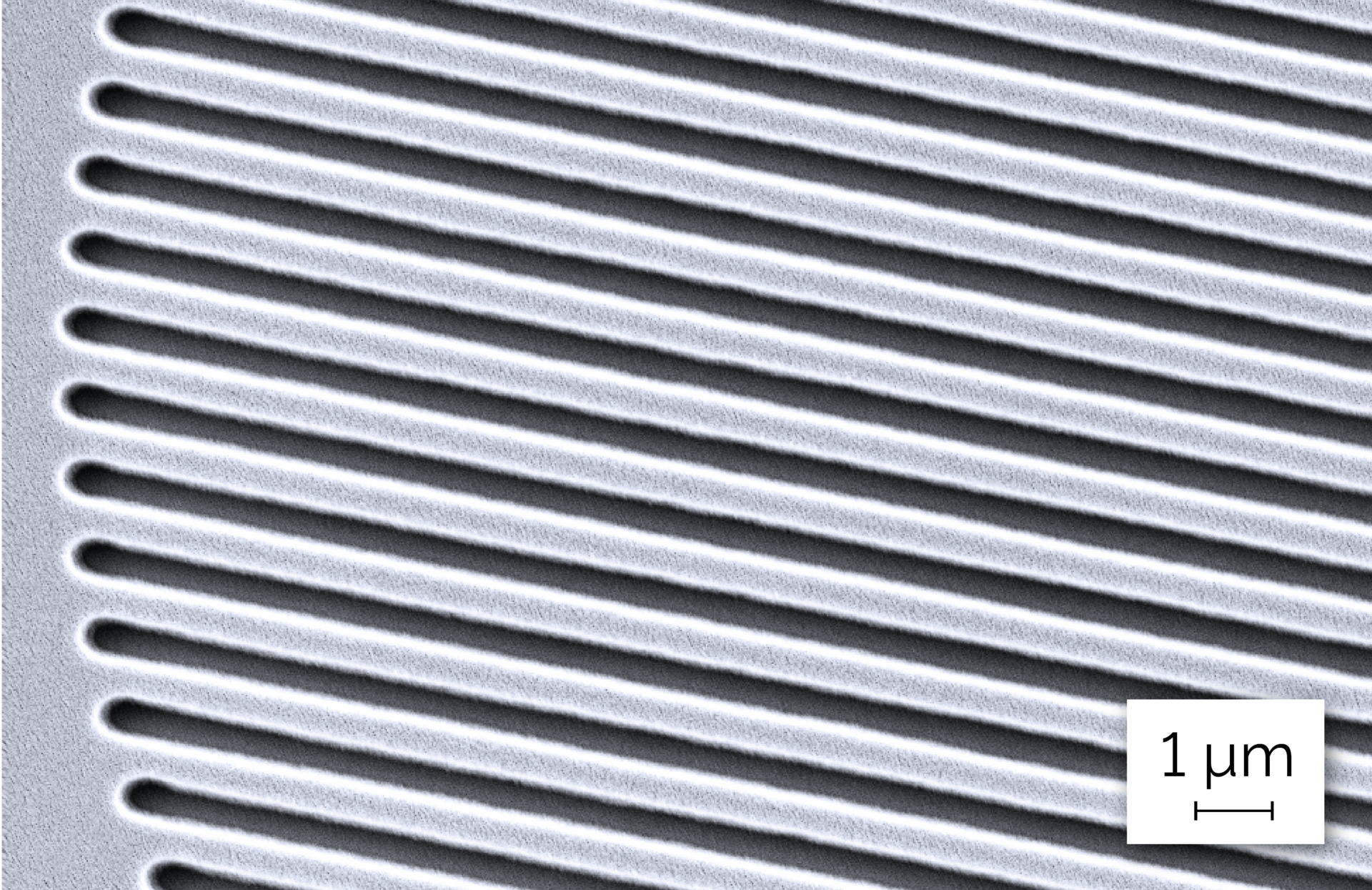
分毫必较,精益求精。ULTRA系统搭载高精度核心组件,确保卓越的对准精度、套刻精度和关键尺寸(CD)均匀性,持续稳定输出高品质掩模版。
-
高精度平台系统:
全气浮平台搭配零热膨胀ZERODUR®载台,提供极致稳定性,彻底消除热漂移。
-
先进的位置控制:
高分辨率差分干涉仪系统,实现特征图形的超精准定位与高重复性。
-
工具匹配功能:
板载校正功能可支持您多台机器精确匹配,确保整套掩模版的一致性。
卓越成像品质和无缝集成
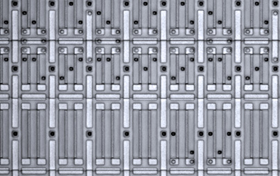
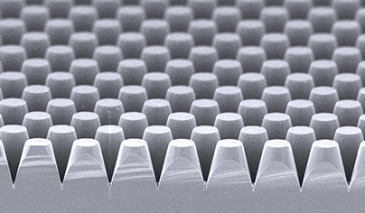
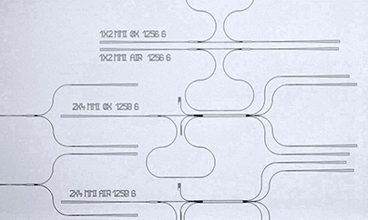
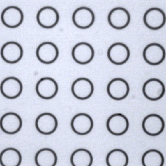
ULTRA系统可制备完美符合严苛标准的无缺陷掩模版,实现500纳米以下特征尺寸的锐利清晰成像。其精心设计确保与现有产线无缝衔接。
-
定制的微納光学器件:
专为掩模版写入优化的定制镜头和低畸变紫外光学设计,确保卓越成像均匀性。
-
占地面积小:
该系统只需占用最小化的净房空间,无需昂贵改造即可快速集成至现有产线。
-
久经考验的可靠性:
ULTRA 是一个全球顶尖掩模版厂共同认证的成熟工具,深受全球行业产能稳定性的信赖。
提升您的掩模版生产
想要了解ULTRA如何缩短生产周期并提升良率?立即联系我们的技术专家,为您量身定制解决方案。。