PRODUCT HIGHLIGHTS
Direct-write Lithography
No mask-related costs, effort, or security risks
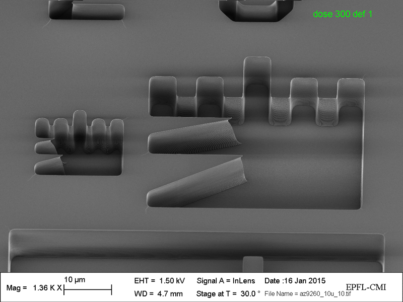
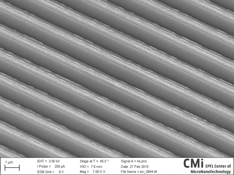
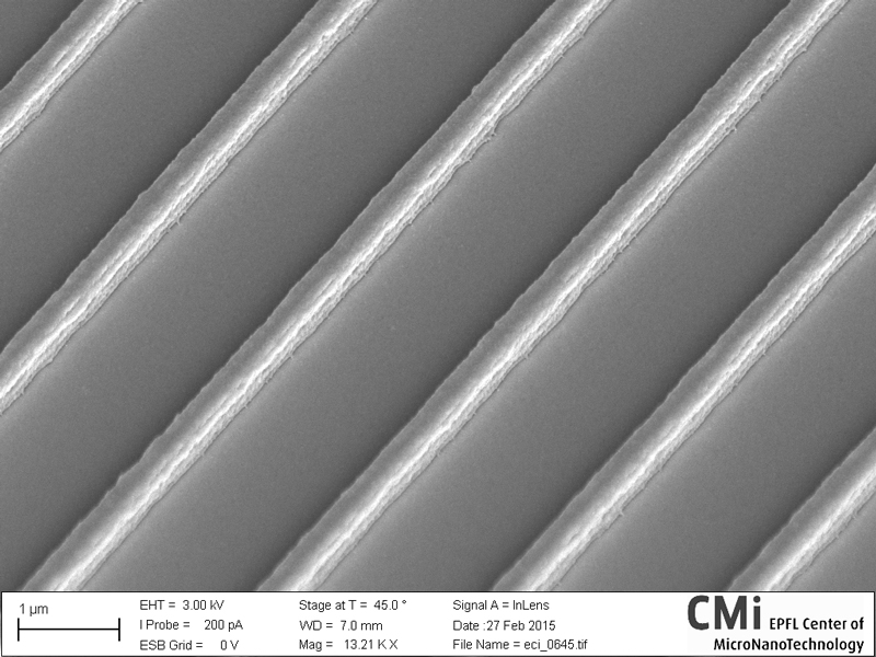
Exposure Quality
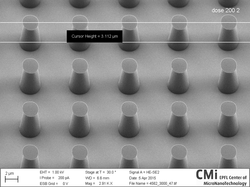
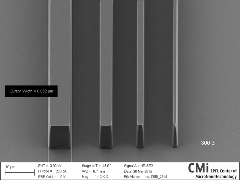
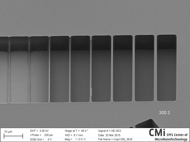
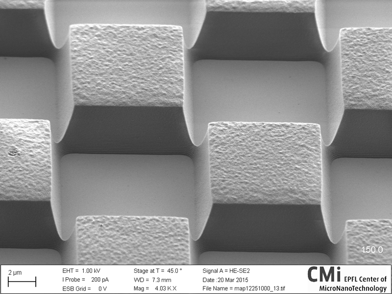
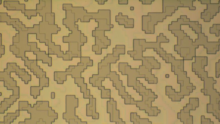
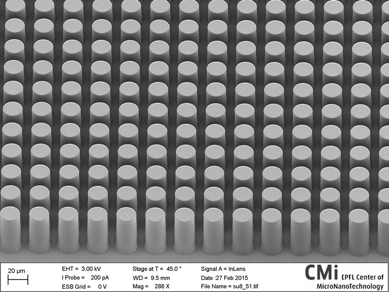
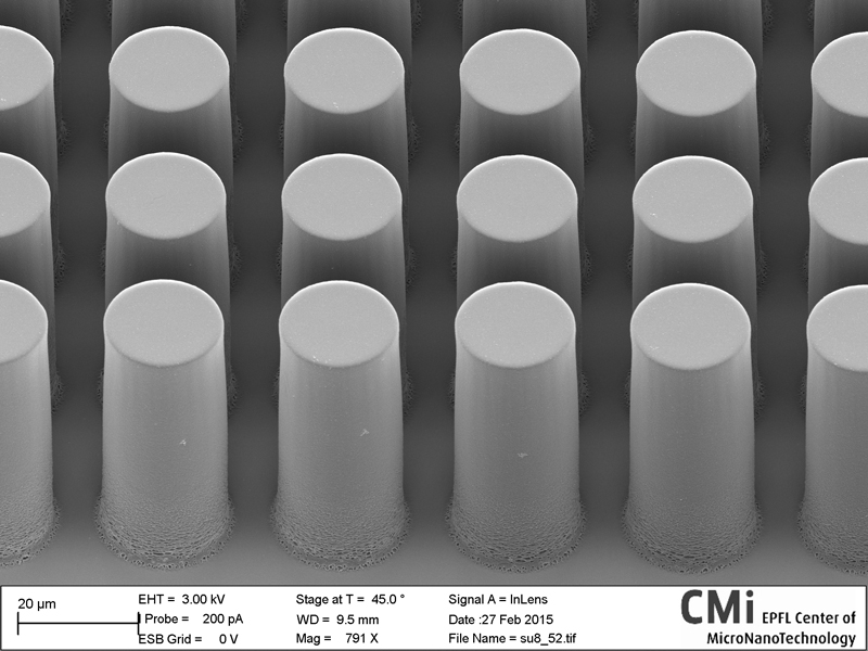
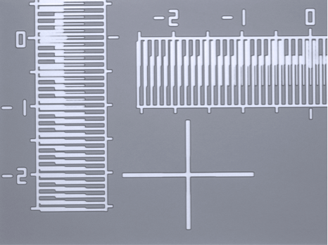
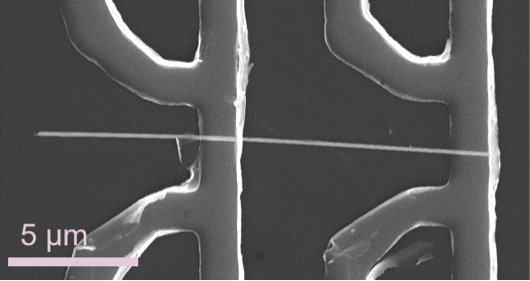
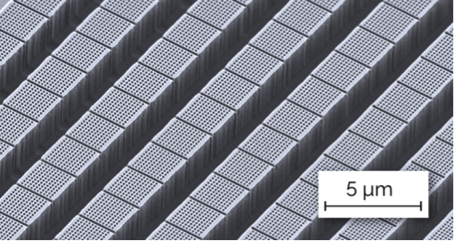
Edge roughness raster mode 100 nm; vector mode 30 nm; CD uniformity 200 nm
Exposure Speed
4″ wafer in 90 minutes
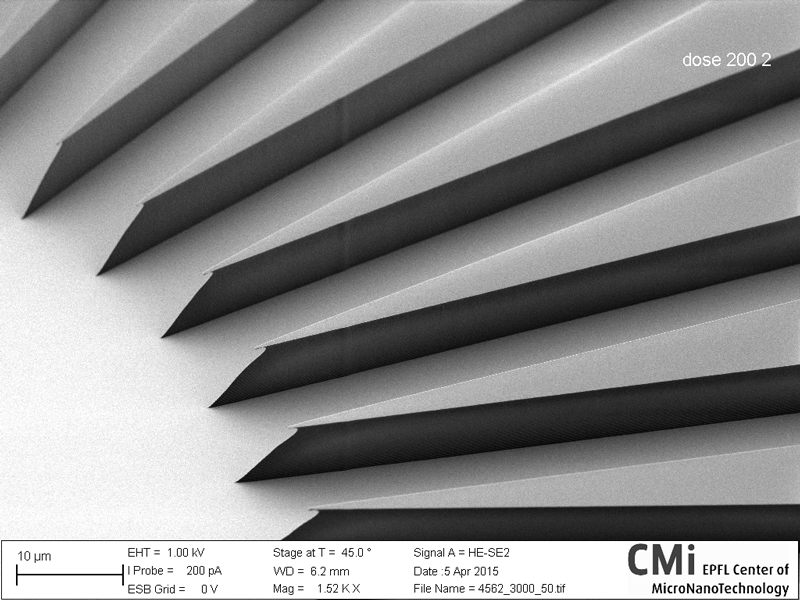
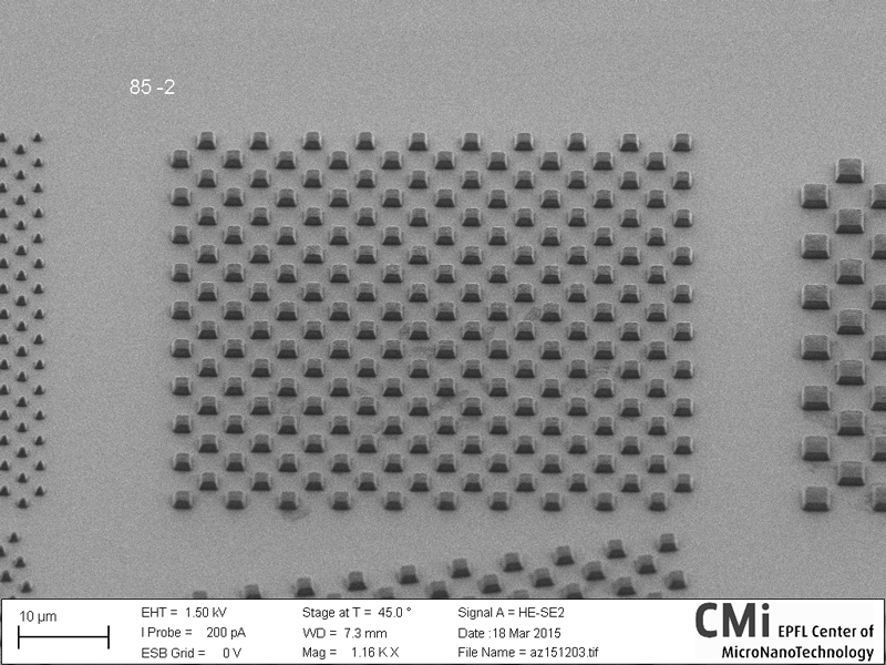
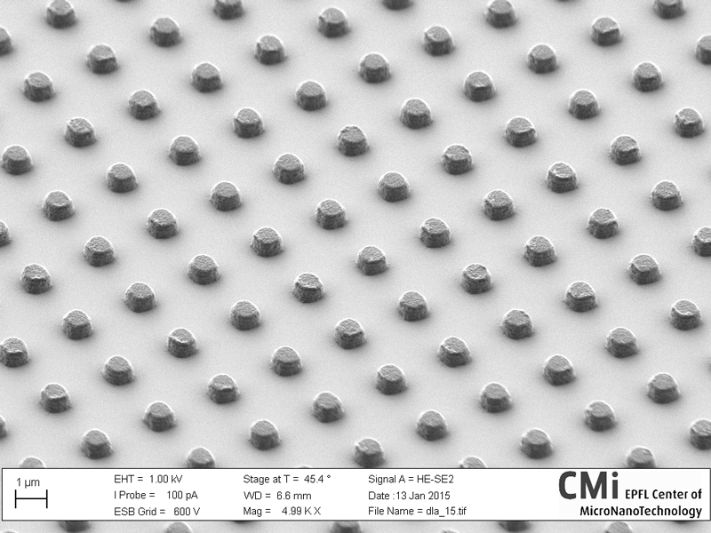
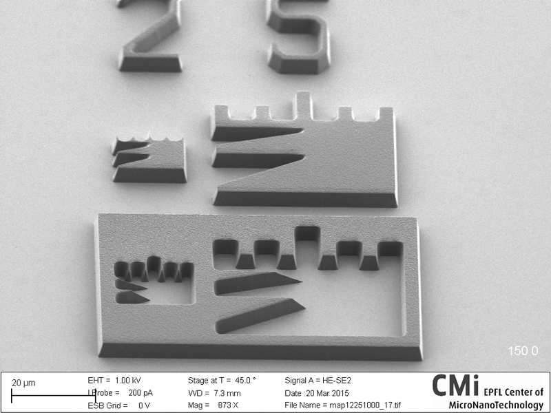
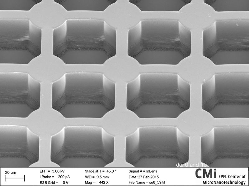
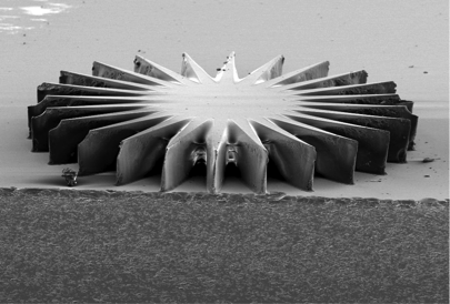
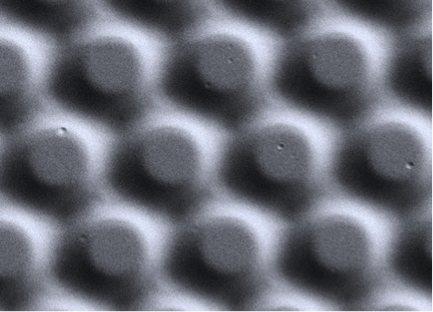
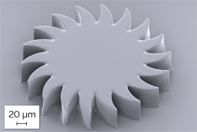
Grayscale Lithography
With up to 256 gray levels, the grayscale exposure capability is part of the standard configuration
Small Footprint
640 mm x 840 mm x 530 mm / 25″ x 33″ x 21″ – the smallest tabletop maskless lithography tool
Flexible Configuration
Choice of exposure wavelength; a choice of Raster and Vector Scan Modules
Flexible Use
Software enables easy switching for variable resolution and throughput speeds
User-friendly
Intuitive software and tool operation; easy handling of small samples
Plug-and-play Setup
Simplified plug-and-play installation reduces overall implementation time and saves costs
多用户实验室的理想之选
用户培训仅需不到1小时
快速准确的对准
250纳米正面/背面对准及误差补偿
卓越的工艺灵活性
双激光并行配置,全面覆盖各类光刻胶
多多种曝光模式可选,兼顾效率与精度
配备专用真空吸盘,轻松应对小型基板、薄膜及翘曲样品
低成本与易维护性
激光寿命长达 10-20 年
直写光刻技术
零掩模版成本,免维护,无安全风险
灰度光刻模式
轻松实现2.5D结构
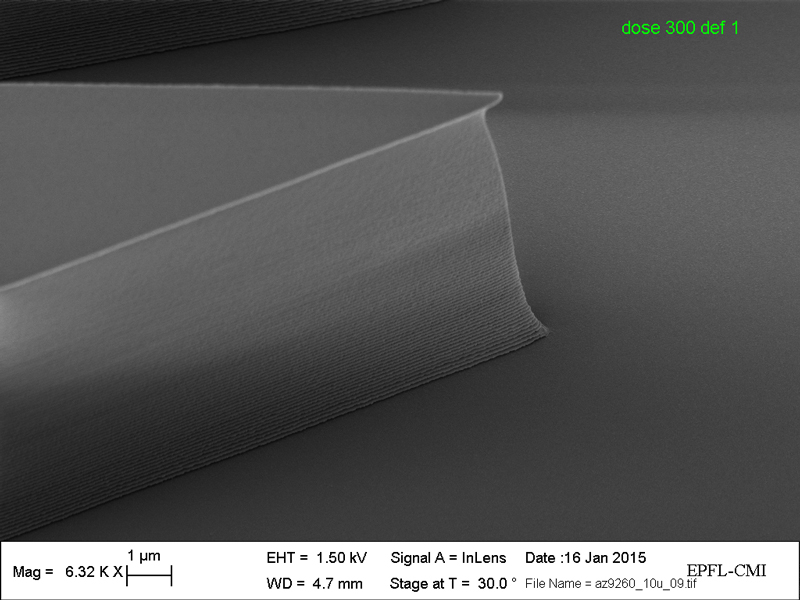
曝光质量
边缘粗糙度60纳米、关键尺寸(CD)均匀性100纳米、自动聚焦补偿翘曲/波纹基板
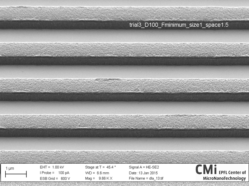
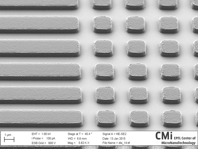
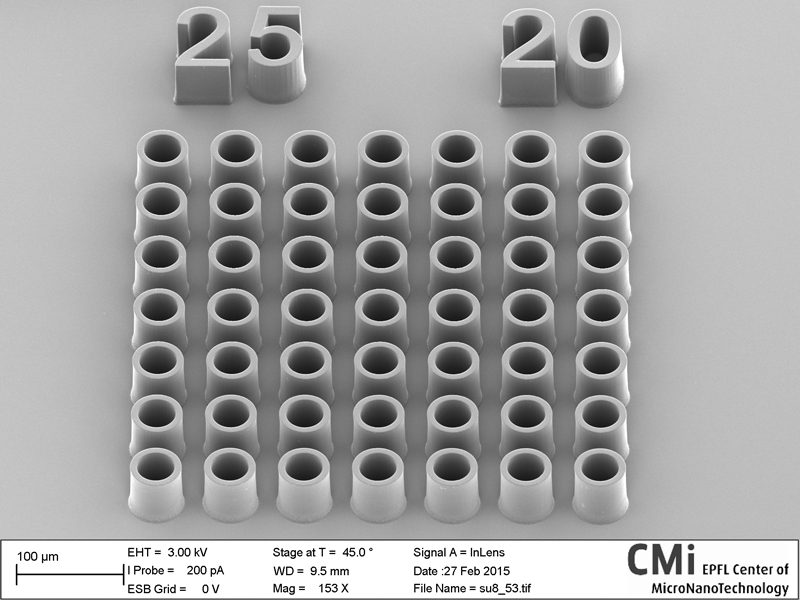
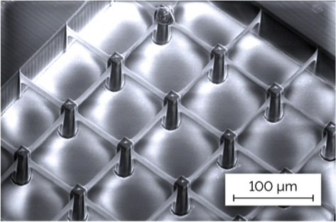
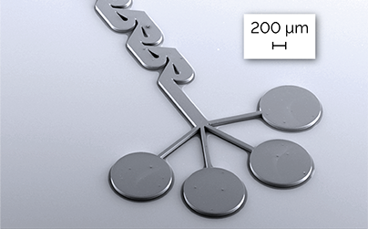
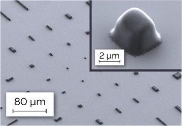
最小特征尺寸
提供两种不同的写入模式,最小特征尺寸可达 0.45 μm
方便用户
专用软件与标准化工作流程,操作直观高效
曝光速度
405纳米激光波长下,150毫米硅片全程<16分钟
Direct-write Lithography
No mask-related costs, effort, or security risks
Flexibility
Direct writing in industrial production allows per-die pattern corrections, e.g. to react to distortions or process variations and serialization
Time-saving
Shorter time from prototyping to production. Digital design management replaces conventional mask librarys
Exposure Quality
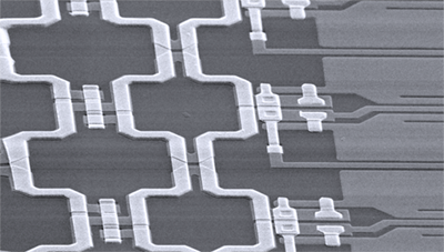
Optical compensation of scaling, rotation; patented substrate tracking technology
Dynamic Autofocus
Superior critical dimensions (CD) uniformity on warped or corrugated substrates
Exposure Speed
300 x 300 mm2 in 5 minutes (write mode 3, two exposure modules)
Full Facility Integration
Customizable automatic loader, substrate chuck including warped substrates, custom workflow “wizards” and interface with manufacturing execution systems (MES)
User-friendly
SEMI-compliant user interface; customized workflow “wizards” for system operators

AVAILABLE MODULES
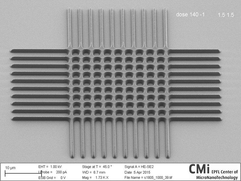
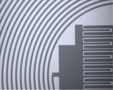
Raster Scan Exposure Mode
Fast with excellent image quality and fidelity; write time is independent of structure size or pattern density. LED light source at 365 nm or 390 nm
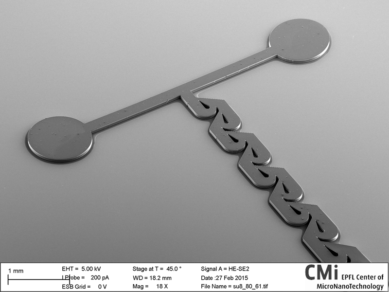
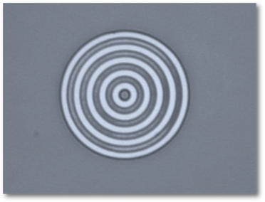
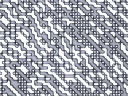
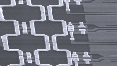
Vector Scan Exposure Mode
Patterning continuous structures consisting of curved lines – where smooth contours are required. Laser light source at 405 nm and/or 375 nm
Three Optical Setups
Min. resolution of 0.6 µm, 1 µm and 3 µm; variable resolution within each mode
Optional Overview Camera
Fast and easy location of alignment marks or other features of interest on substrate
Glovebox Integration
Glovebox for patterning of sensitive materials in a controlled Nitrogen environment
Draw Mode
Import and overlay of BMP files on top of the real-time microscope image — as in a virtual mask aligner; simple lines and shapes can be drawn into the real-time camera image for immediate exposure
Optical Autofocus
Perfect exposure of small samples (<10 mm)
Exposure Area
Can be upgraded from 100 x 100 mm2 to 150 x 150 mm2
Choice of Exposure, Wavelength and Source
Raster Scan Mode: LED light source at 365 nm or 390 nm. Vector Scan Mode: Laser light source at 405 nm and/or 375 nm
Exposure Wavelength
Diode laser sources at 375 nm and/or 405 nm can be mounted
together and used interchangeably to expose different photoresists
Exchangeable Chucks
Additional vacuum chucks for challenging samples like
small substrates, foils, or warped substrates
Customized vacuum chuck layout upon
request
Draw Mode
mport and overlay of BMP files on top of the real-time microscope
image – as in a virtual mask aligner; simple lines and shapes can be drawn into the
real-time camera image for immediate exposure
Autofocus
Air-gauge or optical autofocus for perfect exposure of small samples
(less than 10 mm)
Variable Substrate Sizes
From 3 mm to 6”; up to 8” upon request
Advanced Field Alignment
Automatic field-by-field alignment on individual dies
on the wafer for superior alignment accuracy
Automated Loading Module
SEMI-standard BOLTS plane can be configured for open cassettes or Load Ports for FOUP. The number and configuration of ports can be selected and customized for round or rectangular substrates
Manufacturing Execution System (MES)
Patterning continuous structures consisting of curved lines – where smooth contours are required. Laser light source at 405 nm and/or 375 nm
Backside Alignment
Visual or through-wafer IR backside alignment available with 1 µm positioning accuracy
Exposure Wavelengths
High-power diode lasers with 7 W at 375 nm or 20 W at 405 nm with long lifetime are available
Multipurpose Vacuum chuck
Customized vacuum chucks are available for applications with special substrates (e.g. warped panels)
Service Contracts
Service contract grades for faster on-site support and participation in the spare parts pool