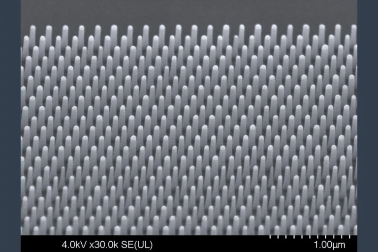
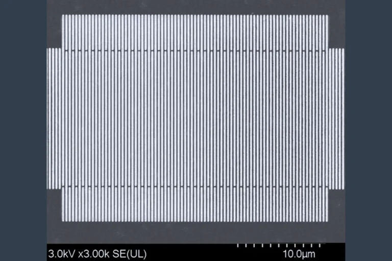
NanoFrazor是一个突破性的热扫描探针光刻(t-SPL)系统,能够在量子器件、1D/2D材料、量子点、Dolan bridges、Josephson junctions和纳米级阵列等各个应用领域进行高端研究。它在复杂应用中表现出色,例如灰度光子学、纳米流体结构、用于细胞生长的仿生基底,以及通过加热进行的任何局部材料改性,包括化学反应和物理相变。
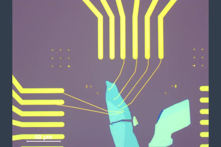
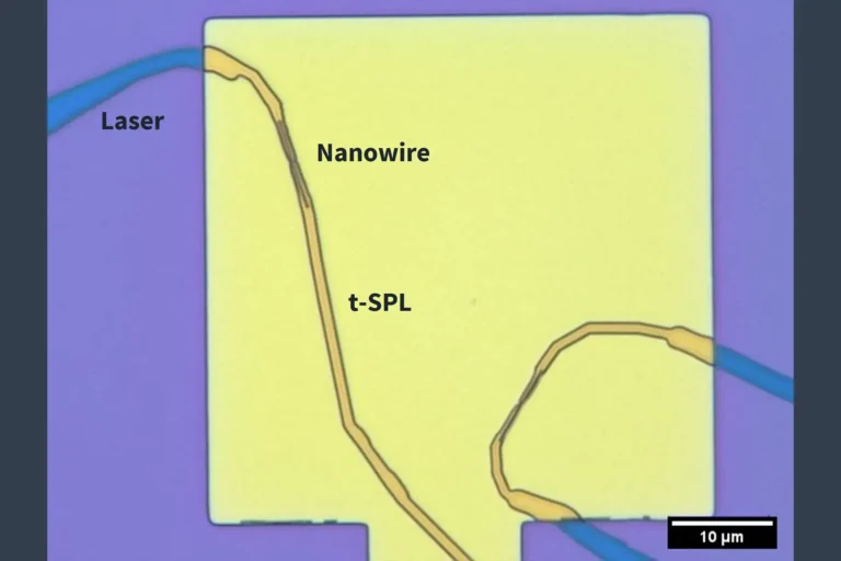
NanoFrazor的核心特点有一个超锋利的可加热探针尖端,可以同时写入和观察复杂的纳米结构;激光直接照射升华(DLS)模块允许在同一个光刻胶中,高效地写入纳米和微结构,并且只需一步制造工艺。
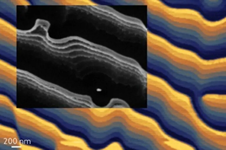
原位成像提供两个独特功能:无标记叠加和在写入过程中比较已写和目标图案,这使得参数可以立即调整。这种称为闭环光刻(CLL) 的方法,使得任何复杂的2.5D(灰度)形状的垂直精度,达到低于 2 nm;快速且精确的控制加热的纳米级探针,使得其他技术都难以实现的创新成为可能。
NanoFrazor来自于IBM Research Zürich(苏黎世研究院)超过20年的研究发展,如今在Heidelberg Instruments Nano推进硬件和软件技术,继续不断进步。我们的专家优化蚀刻和剥离等图案转移工艺,以适应各种应用需求,并将这些专业知识编入全面的最佳实践和数据库,以支持我们的客户。
基于模块化平台,NanoFrazor可以根据特定应用和实验室环境进行定制。图案化模式、外壳选项和软件模块可以组合,以实现最佳功能、占地面积和灵活性。随着研究的发展,可以添加升级和附加模块,确保NanoFrazor能够适应不断发展的需求。
NanoFrazor彻底改变了纳米制造技术,使复杂的热探针扫描光刻技術(t-SPL)成为突破性研究和技术进步的可行工具。
为了提供对新世代NanoFrazor模型的更详细视角,该模型首次于 2024 年 5 月推出,我们已发布专门的网站,您可以在此了解更多信息并配置您的系统:nanofrazor.com。
为什么客户选择我们的系统
「NanoFrazor在纳米光刻领域提供了独特的功能组合,集成在一台仪器中。我特别强调它在无标记叠加和对二维材料低损伤的拼接方面的优势,以及在三维灰度纳米光刻和材料通过加热转换和改性方面的应用。」
— Francesco Buatier de Mongeot
实验凝聚态物理教授
意大利 热那亚大学物理系
The NanoFrazor is a groundbreaking commercial system for Thermal Scanning Probe Lithography (t-SPL), enabling advanced research in various application areas such as quantum devices, 1D/2D materials, quantum dots, Dolan bridges, Josephson junctions, and nanoscale arrays. It excels in complex applications such as grayscale photonics, nanofluidic structures, biomimetic substrates for cell growth, and any local material modification through heat, including chemical reactions and physical phase changes.
At its core, the NanoFrazor features an ultra-sharp, heatable probe tip that writes and inspects complex nanostructures simultaneously. The Direct Laser Sublimation (DLS) module allows nano- and micro-structures to be written into the same resist layer efficiently in a single fabrication step.
In-situ imaging enables two unique features: markerless overlay and comparison of the written and target patterns during writing, in such a way that the parameters can be immediately adjusted. This approach, called Closed-Loop Lithography (CLL), results in sub-2 nm vertical precision for 2.5D (grayscale) shapes of any complexity. Fast and precise control of a heated nanoscale tip enables innovation not otherwise feasible with other techniques.
Developed from over 20 years of R&D at IBM Research Zürich and now at Heidelberg Instruments Nano, the NanoFrazor continuously advances in hardware and software. Our experts refine pattern transfer processes like etching and lift-off for various applications, compiling expertise into a comprehensive library of best practices and protocols to support our customers.
Built on a modular platform, the NanoFrazor can be tailored to fit specific applications and laboratory environments. Patterning modes, housing options, and software modules can be combined for optimal capabilities, footprint, and flexibility. Upgrades and additional modules can be added as research evolves, ensuring the NanoFrazor adapts to advancing needs.
The NanoFrazor revolutionizes nanofabrication, making sophisticated t-SPL accessible for groundbreaking research and technological advancements.
To provide a more detailed perspective to the new NanoFrazor model, introduced first in May 2024, we have published a dedicated website, where you can learn more and configure your own system: nanofrazor.com.
WHY CUSTOMERS CHOOSE OUR SYSTEMS
"The Nanofrazor offers a unique combination of features in a single compact instrument for nanolithography. I highlight in particular markerless overlay and stitiching with low damage on 2D materials, 3D grayscale nanolithography, and direct thermal conversion and modification of materials."
Francesco Buatier de Mongeot, Professor of Experimental Condensed Matter Physics
Dipartimento di Fisica, Università di Genova
Genova, Italy