DWL 66+ 具有无与伦比的多功能性、专业级灰度功能以及市场上所有直写激光系统中最高的分辨率。
作为一个高度通用的系统,DWL 66+ 专为微机电系统、微电子、微流体、传感器、光学、光子学、光伏、材料科学、量子设备等领域的研发和快速原型设计而设计,几乎适用于任何需要微结构制造的应用。
主要功能
-
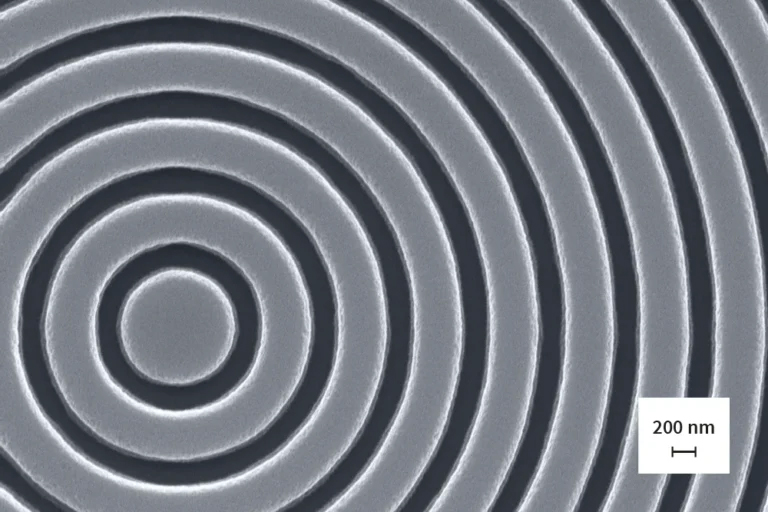
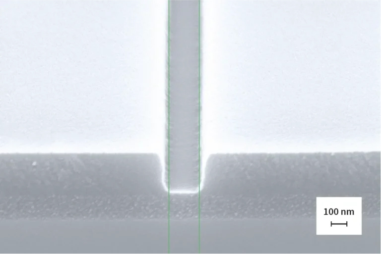
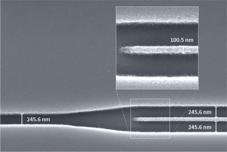
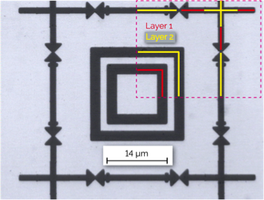
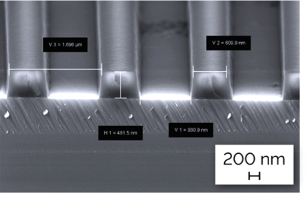
200 纳米最小特征尺寸的高分辨率模式
我们的写入模式 XR 可提供无与伦比的分辨率、质量和速度组合。
-
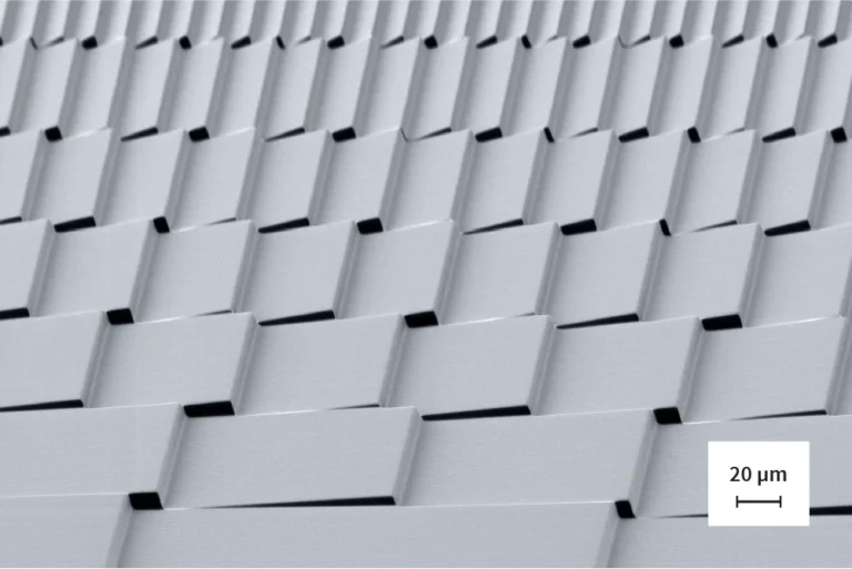
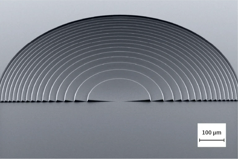
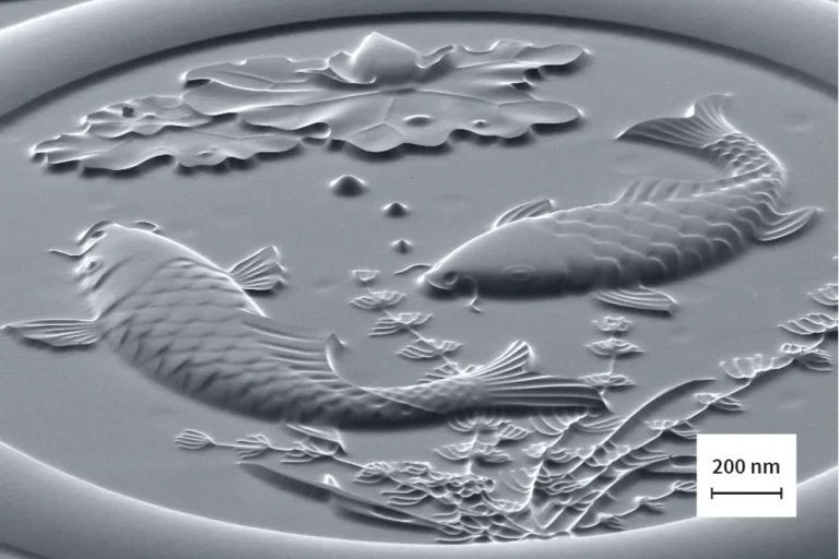
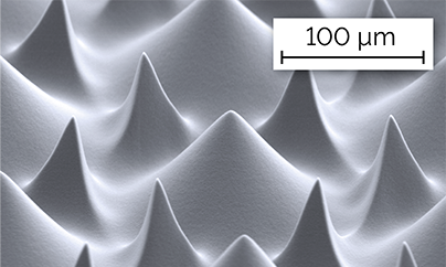
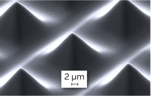
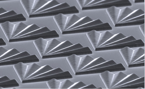
65,536 级灰度光刻
可在厚度达 150 µm 的光刻胶中进行灰度光刻,并具有出色的表面质量。
-
完全可定制的系统配置
30 年的持续开发和 400 多台已安装设备,使 DWL 66+ 成为市场上功能最全面、最成熟的系统。
将光学光刻技术提升到一个新水平
DWL 66+ 不仅仅是掩模对准器的替代品,它还是一种升级产品,能将精度、分辨率和结构保真度提高到一个新的水平。这种无掩模系统将大大缩短开发新设备所需的时间,并带来新的可能性。
-
即时更改设计
修改 CAD 文件并立即开始曝光。没有与掩模相关的成本、工作量、等待时间或安全风险。
-
多种基底兼容性
DWL 66+ 不仅能在标准芯片或晶圆上曝光,还能在任何材料、尺寸、厚度或形状的基底上曝光,包括曲面。
-
减少电子束光刻系统的工作量
在许多情况下,DWL 66+ 可以执行以前需要电子束光刻系统才能完成的曝光,从而将电子束解放出来,用于要求更高的任务。
毫不妥协的曝光质量
DWL 66+ 是专为研发而设计的,但它采用了我们工业生产系统的核心技术,以确保最高水平的精度和可重复性。
-
受控环境
DWL 66+ 系统包括一个层流箱,可最大限度地减少微粒污染,并确保暴露期间的热稳定性。
-
干涉位置控制
高分辨率干涉仪与实时光束位置校正相结合,确保了图案放置的准确性和结构的真实性。
-
实时自动对焦系统
DWL 66+ 包括常见的光学自动对焦系统,但通过专有的辅助自动对焦系统进行了增强,该系统的功能独立于光学反馈。这样,即使在透明或低反射率基底上也能实现精确对焦。
质量与生产率的优化组合
DWL 66+ 不会为了提高产量而降低曝光质量。写入速度为最高质量设置,写入时间不取决于曝光区域内的填充系数、形状或结构数量。
-
可交换写入模式
轻松切换写入模式,优化分辨率和吞吐量,满足您的应用需求。
-
专有软件和硬件
直观的用户界面,加上优化的设计准备和快速的数据转换,实现了从设置到曝光的快速工作流程。
-
全自动化
DWL 66+ 的操作可通过自动正面或背面校准以及盒到盒处理系统实现全自动化。
DWL 2000GS和4000 GS 激光直写系统具有快速、灵活的高分辨率,能够达到灰度光刻的专业表现。灰度光刻能够在厚度较大的光阻中创建复杂的2.5D微结构。灰度光刻模块的最常见应用包括制造用于通信或微光機電的晶圆光学组件;也被用于显示器制造和生医科学设备的制造。
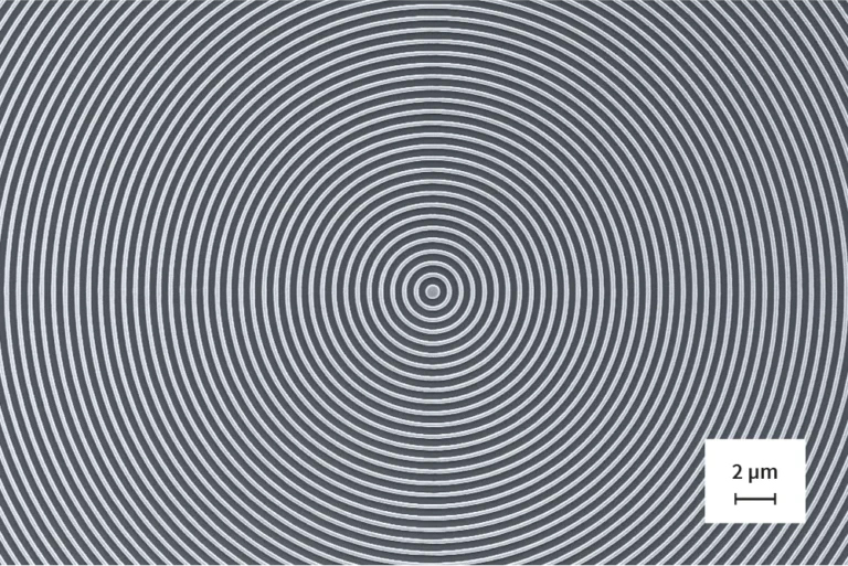
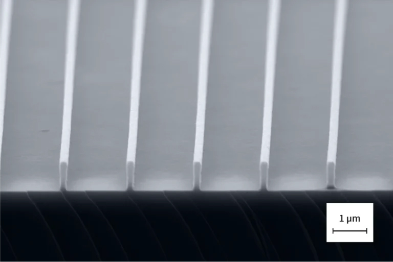
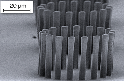
除了灰度光刻外,DWL系列还能以最高分辨率的500 nm最小特征大小进行二进制2维光刻。这些系统提供了完美的解决方案,如果您需要在微机电(MEMS)、BioMEMS、微光学、集成电路(ASIC)、微流道、传感器和全息图等领域中,对掩膜版或芯片进行高通量的图案,它们的书写区域可达400 mm x 400 mm,并带有选配自动加载系统。
The DWL 2000 and 4000 laser lithography systems constitute fast, flexible high-resolution pattern generators, capable of the Professional performance level of Grayscale Lithography. The latter allows the creation of complex 2.5D structures in thick photoresist over large areas. Most common applications of the Grayscale exposure mode include the fabrication of wafer level optics used for telecommunication or illumination market segments; it is also used in display manufacturing, and in device fabrication in Biology and the Life Sciences.
In addition to Grayscale, the DWL series tools excel at binary 2D exposures, down to the highest resolution with a minimum feature size of 500 nm. With a write area of up to 400 mm x 400 mm and the optional automatic loading system, these systems provide the perfect solution if you require high-throughput patterning of masks and wafers in MEMS, BioMEMS, Micro Optics, ASICs, Micro Fluidics, Sensors, and CGHs.